


an127: Op-Amp Errors, Another View
Application Note
Preamble
The subject of Op-Amp errors has been covered by many writers. Dataforth’s Application Note 102 [1] covers the topic as applied to instrumentation amplifiers and provides links to spreadsheets for worst case error analysis. This is a good place to go for the practical engineer. The instrumentation amplifier of Application Note 102 can be decomposed into the non-inverting amplifier of this application note using Bartlett’s bisection theorem [2].Using circuit simulators and suitable Op-Amp macros will provide quick results. Two free downloads are TI Tina and LTspice. These may be found on the websites of Texas Instruments and Linear Technology.
This note concerns only Op-Amps and does not attempt to be exhaustive. Its objective is to show how final equations of some basic errors are derived from first circuit principles – primarily node analysis. Final equations are enclosed with a box.
This Application Note is for the math driven reader. We have all had the experience in our math and technical education of reading a treatment of some topic where the author introduces material and jumps to a final equation stating “the derivation is left to the interested reader.” Unless our teacher gave the derivation as an assignment, most of us were not interested. Another hated statement is “may be seen by inspection.” Not all students are interested inspectors. It does have to be admitted that many books would be much too long if not for these shortcuts. It is also true that self-taught knowledge, while frequently incomplete, often stays longer. Perhaps nonmath oriented people never knew that following along with pencil and paper is what makes math come alive. For many, math becomes a blur of meaningless symbols, mindless formula plugging, or even blind imitation.
An elegant way to do the following analysis is using Middlebrook’s Extra Element Theorem [3] However, I start with basic circuit analysis and turn the algebraic crank.
Offset Voltage
Assume the circuit of Figure 1 is the “Ideal Operational Amplifier” except for offset voltage and finite open loop gain.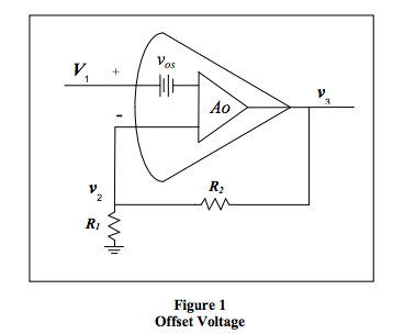
First, the ideal amplifier. For Αo to be very, very large, the independent variable V1 must be close enough, for all practical purposes, to the dependent variable ν2. To find the Ideal Amplifier Gain, use the voltage divider relation:
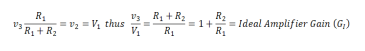
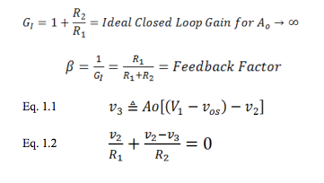
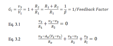
Negative feedback amplifiers are said to have closed loop gain (Gcl). When the feedback connection is not made, the phrase becomes open loop gain (Gol ). R1/R1 + R2 is called the feedback factor. In this note Β symbolizes the feedback factor.
Rearranging the terms,
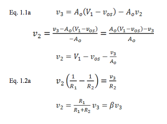
Combining Eq. 1.1a and Eq. 1.2a,
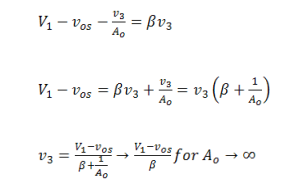
Equation 3 easily, perhaps eloquently, shows how offset voltage and limited open loop gain modify the familiar ideal gain equation. Modern Op-Amps have very high open loop gain. If , Αo → ∞ the error of offset voltage alone is easily observed. It is multiplied by the closed loop, ideal gain. This is often the most serious problem in high gain Op-Amp applications.
Note that this is really basic feedback theory and applies to much more than just Op-Amps. Some communication amplifiers and various control problems are examples with open loop gain far from infinite.
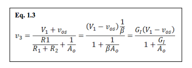
Bias and Offset Current
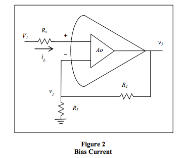
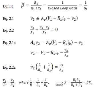
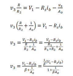
Eq. 2.1a and 2.2a
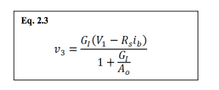
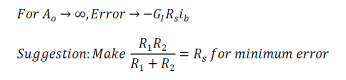
For many modern Op-Amp applications, the ideal model is adequate. When it is not, consideration of offset voltage and input current suffices for many of the rest. Exceptions are high gain circuits and power amplifiers driving a heavy load. Note that integrated circuit OpAmps have almost equal bias currents on the positive and negative inputs. The difference is sometimes called offset or difference current. If the source resistances as seen from each input are nearly the same, the error is minimized.
The rest of this paper is for the interested reader. It has more importance in general control systems.
Output Resistance
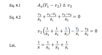
The following amplifier is ideal in every way, except it has limited open loop gain and a non-zero output resistance. As we will see, if we assume infinite open loop gain, the output resistance would have no effect. Since we are considering non-zero output resistance, a load resistance is included. Of course, the gain determining resistors are also a load on the amplifier.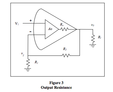
Gathering terms,
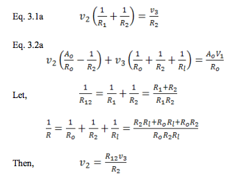
Combining equations,
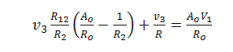
Or,
Rearranging terms,
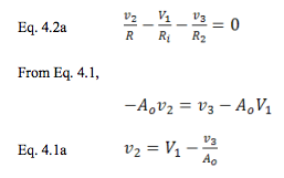
Combining equations 4.1a and 4.2a,
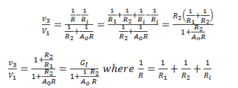
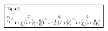
From equation 4.3, we can easily see how changes the “ideal gain.” For infinite Αo, Ri has no effect whatsoever. For that reason, we have to consider both in the same model. This is intuitively satisfying from merely looking at Figure 4. If we let Ri approach infinity, we get the effect of Αo alone.
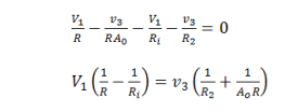
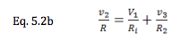
Now we can consider the input resistance of the entire circuit.
From this we can see that the input resistance of the OpAmp is increased by the ratio of open loop gain to the closed loop, “ideal gain.” For example, using typical values 105/102 = 103 gives an increase multiplier of 1000. Note that “ideal gain” is the inversion of the feedback factor:

Some authors often use , rather than a symbol for “ideal gain.”
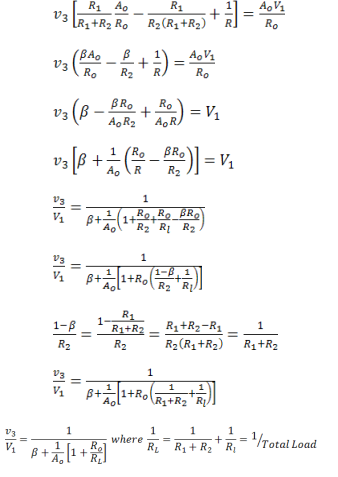
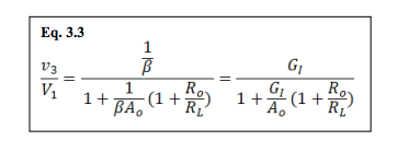
Input, Output, and Load Resistance Altogether
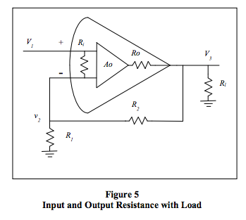
Define:
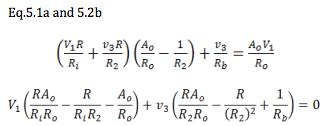
Now, we have a clear relation between the dependent variable ν3 and the independent variable V1. At this point, I will take the easy way out and say the next intermediate steps are “left to the interested reader.” The same algebraic methods of factoring and cancelling used above will get you to Eq. 5.3. Remember as you go that Αo, Ri, and Rl must be allowed to clearly approach infinity. So put them in denominators so those terms will approach zero. Ro must approach zero, so put it in numerators. Finally look for any way that negative terms can cancel out.
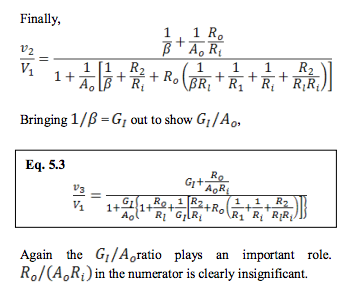
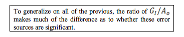
From equation 5.3, you may easily see how the amplifier imperfections can go to their ideal limits leaving the ideal gain equation, and there are no vexatious negative signs. Equations with a negative sign cause me to wonder if the whole thing could go negative. Then I have to ask myself if that is physically meaningful or possible. If not, I may have made a mistake. Last of all, don’t forget unit analysis. Gain equations must have all terms unit-less, voltages volts, resistances resistance, and so on. This is often a quick way to see something is wrong, or going wrong, in a derivation.
Example and Conclusion
Let’s see if any of this is worth considering. Consider the following design.
Αo = 200k
Ri = 50kohm
Ro = 100
R2 = 99.9k
R1 = 100
Rl = 2k
Ri = 50kohm
Ro = 100
R2 = 99.9k
R1 = 100
Rl = 2k
These numbers in equation 5.3 yield a gain of 994.76, a 0.52% gain error. Almost all of this comes from the denominator, and there only from Α0. A very slight amount comes from the ratio Ro/Rl. I believe we could also calculate an error for one element at a time and assume superposition. Beyond this 0.5% error, the resistor tolerances are obviously important. Offset voltage and bias current may produce larger errors and should usually be considered first. Additional error sources are noise, power supply rejection, and common mode rejection. Noise is a whole subject in itself. Then comes temperature stability and ageing. Room temperature errors can be calibrated out, but temperature and ageing cannot, unless we use some type of reference and do automatic calibration with a feedback loop. If we don’t have a processor for this, a clocked feedback integrator with an analog multiplexer can be used for offset error. Just provide feedback to the ground connection of with R1 an inverting integrator. Be careful of noise.
Perhaps for day-to-day work it is best to just use a good simulation! However, always a however, while quick numerical modeling is a great aid, we easily lose insight into the sources of error. Equations like 5.3 can show where the bulk of error comes from for a particular application. In the example, almost all of the gain error comes from the limited open loop gain and resistor tolerances.
References
- Dataforth Application Note AN102
http://liwww.dataforth.com/catalog/pdf/an102.pdf - Bi-section theorem: Bartlett, AC, “An extension of a property of artificial lines,” Phil. Mag., Vol. 4, P902, Nov. 1927
Was this content helpful?
Thank you for your feedback!