

AN103: Common Mode Voltage
Application Note
Preamble
Signal conditioning modules typically have two types of front-ends; either single ended (SE) or differential ended (DE) inputs. Single ended signals are referenced to the module's power supply common, which should be at the reference potential of the signal being measured. If this reference is not zero potential, then the actual input signal includes an unwanted voltage, which is amplified along with the desired differential signal producing serious errors on the output.
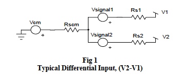
Differential ended inputs are simply two SE inputs referenced to a common potential where the "information" signal is the difference between these two SE inputs. Signal conditioning modules must use differential input front-ends to amplify the difference between two SE input signals. Any non-zero potential on the reference is common to both SE inputs. Figure 1 illustrates that neglecting all source resistors; V2 is Vcm+Vsignal2 and V1 is Vcm+Vsignal1. Note, (V2-V1) is (Vsignal2-Vsignal1).
In theory, differential measurements eliminate the effects of common mode voltage (Vcm). Unfortunately, all differential amplifiers have two gains; a differential gain (Ad) and a common mode gain (Acm). Moreover, the value of these gains depend upon the output connection; either single ended (SE) or differential ended (DE)
This application note discusses the internal origin of IC differential amplifier common mode gain (Acm) and some of the external applications that create common mode voltages. For the reader who is not particularly interested in the theory of Acm; he/she may skip to the section on Examples.
Figure 2 is a simplified basic MOS differential pair, used in many instrumentation amplifiers.
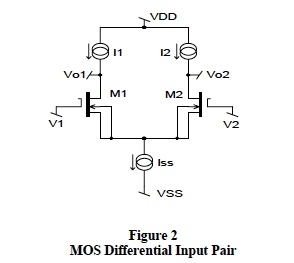
Figure 3 is a simplified dynamic model of the MOS differential pair shown in Figure 2. Current sources I1, I2, Iss are represented by Rd1, Rd2, Rss respectively. Gm1, Rds1 and Gm2, Rds2 model the MOS devices M1, M2 respectively.
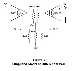
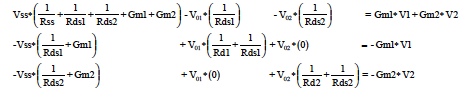
The solution to a set of node equations written at Vss, Vo1, and Vo2 will provide expressions for the individual output voltages, Vo1, Vo2. These symbolic expressions are mathematically very messy. However, if one assumes M1, M2 and I1, I2 are identical, these expressions simplify substantially. Moreover, if Rd1=Rd2 ≡ Rd; Rds1=Rds2 ≡ Rds; and if 21, then
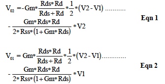
The assumptions made in developing Equations 1 and 2 are not always completely possible; however, they provide the reader with an insight into the parameters responsible for establishing "gains". Equations 1 and 2 are single ended (SE) output expressions with two terms;
- a gain term multiplying the differential input, and
- another gain term multiplying the SE input voltage. Note: This common SE term is the origin of common mode voltage gain.
Instrumentation amplifiers typically have several internal differential pairs, all of which contribute to developing the final SE output, which includes a net common mode gain term. Designers and manufacturers of IC instrumentation amplifiers use two techniques to diminish this common mode term;
- ensure internal differential pairs have matched devices, and
- use topologies that use large dynamic values of Rss.
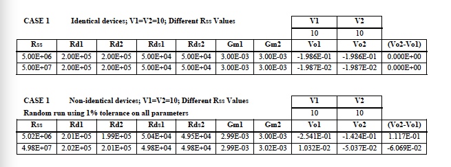
Case 1: Identical devices with 10 volts of common mode voltage, two different Rss values of 5 MegΩ and 50 MegΩ show that;
- SE outputs do have a common mode gain, which decreases as Rss increases.
- There is no DE output, (no common mode gain).
- SE outputs do have a common mode gain that decreases as Rss increases.
- There are DE outputs; consequently, a common mode DE output gain exists.
Practical Examples of Common Mode Voltages
Figure 4 illustrates a typical field sensor that generates a net differential signal and includes both the sensor common mode voltage source (Vcm, Rscm) and a common mode voltage source (Vx, Rx) contribution from the difference between the field ground and data acquisition system ground.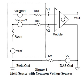
The wiring between a field sensor and its associated signal-conditioning module is subject electro-magnetic induced voltages. These induced voltages can add both an additional common mode voltage source and a differential input error voltage. Analysis of this phenomenon is beyond the scope of this document. Figure 5 illustrates two different topologies for measuring load currents using shunt resistors.
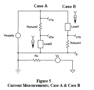
Case A is a differential voltage (V1a/V2a) measurement across a shunt inserted in the supply line. In this case, the common mode voltage is equivalent to the supply voltage plus the voltage difference between the field ground and DAS ground.
Case B is, again, a differential voltage (V1b/field-ground) measurement across a shunt inserted in the field ground line. A differential measurement is recommended here to eliminate the error caused by the common mode voltage equivalent to the voltage difference between the field ground and DAS ground. Figure 6 illustrates a standard bridge sensor, which is often the basis for industrial measurements.
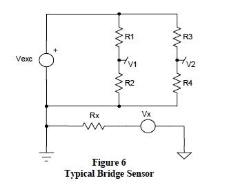
For the typical bridge sensor shown above, the differential output voltage (V1-V2) there has an inherent common mode voltage, which is typically 1/2 the excitation voltage with an additional common mode voltage component equivalent to the voltage difference between the field ground and DAS ground.
Avoiding Errors Due to Common Mode Voltages
Common mode voltages are inevitable in practical industrial measurements. An instrument engineer should always use;- differential measurements and
- signal conditioning modules with high CMR
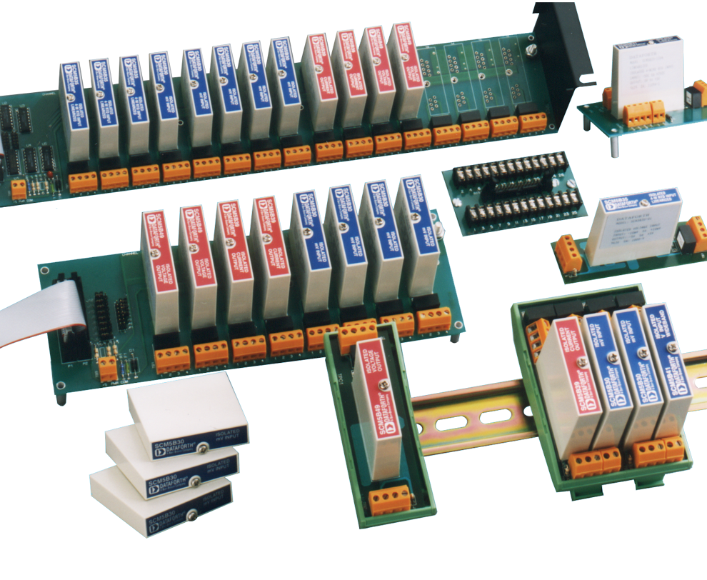
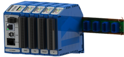
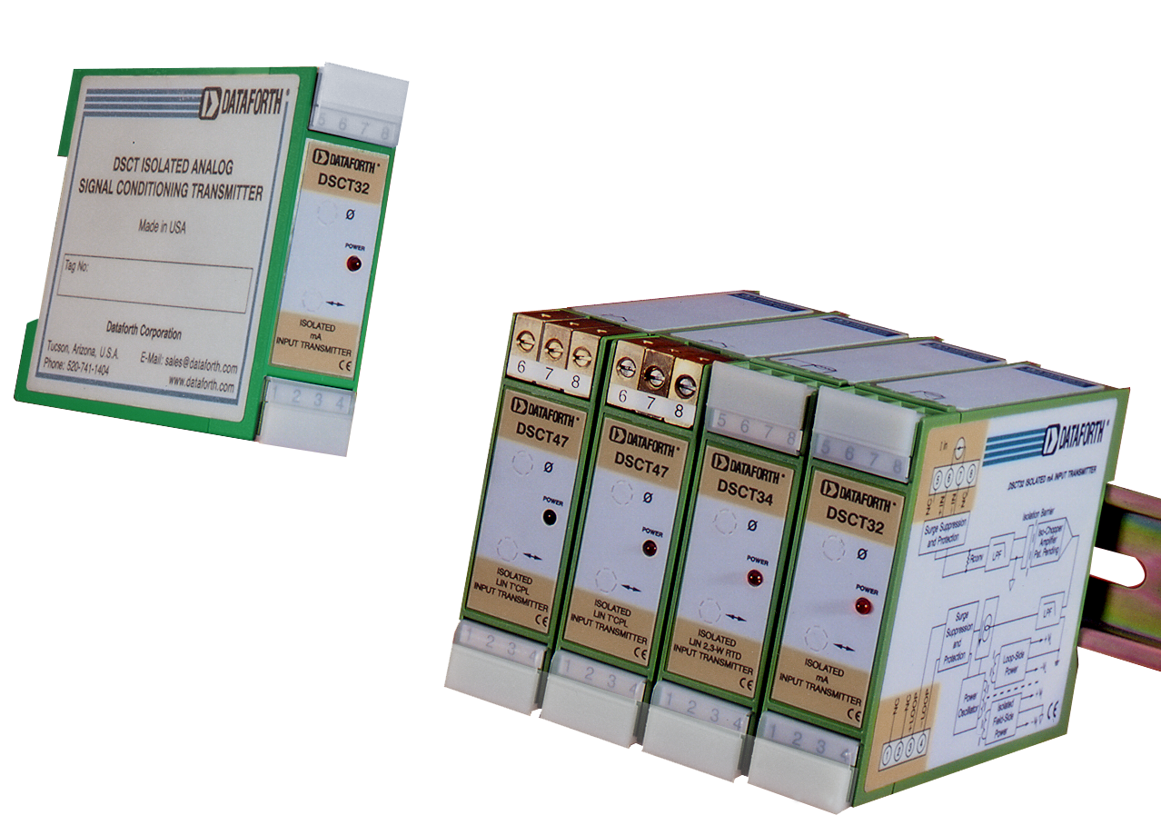
DATAFORTH MEASUREMENT DEVICES
Dataforth has a unique patented Isochopper Amplifier front end, which employs a transformer isolation barrier with a unity gain amplifier resulting in CMR specifications independent of module gain. Many electronic amplifier manufactures typically specify common mode rejection (CMR) referred to the input (RTI), which means that common mode voltage errors are determined by; Verror = [Vcm÷(10CMR/20)]∗(Module Gain). Dataforth's specification for CMR is independent of gain; therefore, common mode voltage errors in Dataforth's modules are determined by; Verror = [Vcm÷(10CMR/20)] ! The reader is encouraged to visit Dataforth's website www.Dataforth.com for detail information on all Dataforth's product.Figure 7 is a block diagram of Dataforth's SCM5B30/31 Analog Voltage, Narrow Bandwidth Input Module. This module has a 1500 Vrms continuous common mode voltage rating with a CMR of 160 dB. Using this module to measure a differential voltage with an associated common mode voltage (Vcm) will produce an output common mode error equal to Vcm∗10E-9 volts. For example, a common mode voltage of 100 Volts would create an output error of 1 μVolt.
Using Dataforth’s SCM5B31 Narrow Bandwidth Analog Input Voltage Module
Figure 8 illustrates an Aluminum electrolytic reduction cell, which employs currents on the order of 50,000 to 150,000 amperes that eventually erodes these carbon electrodes. The voltage between electrodes is an indication of their condition and is used by plant maintenance personnel to determine when electrodes must be replaced.. A Dataforth SCM5B31 module is ideal for this electrode voltage measurement application.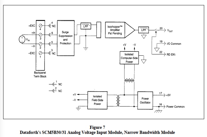
Dataforth's SCM5B30/31 Analog Voltage Input Module, Narrow Bandwidth Module
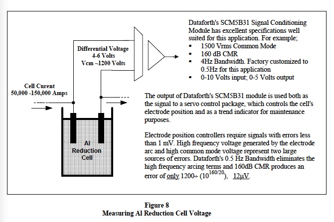
Table 1 Simple Differential Pair Analysis of Topology in Figure 3 An Excel table similar to Table 1 is available on spreadsheet #1 of an interactive Excel Workbook from Dataforth's Web site. The reader is encouraged to download this Excel file Differential Pair Simulation with Simple Device Model (Gm, Rds, Rd, and Rss), choose their own values, follow instructions, and examine the effects of their own selected values.
Download PDF
Download a PDF version of this content.