

an502: SCM5B Ground Connections and Host System Interfaces
Application Note
Use of the ground jumper arrangement on the SCMPB01 and SCMPB02
backpanels depends on the particular host analog-to-digital converter (ADC)
system connected to the backpanels and SCM5B modules. This application note
details four common system interface schemes; more than these could exist. The
SCMPB02 multiplexing backpanel is used as the example rather than the
SCMPB01 because it has more logic circuitry which depends on proper
interface schemes. However, most of the following notes are applicable to both.
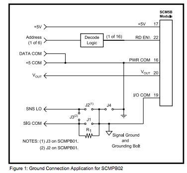
CASE 1: Factory Configuration:
This is a general purpose configuration which may be used with single-ended or differential ADC systems. For single-ended ADC systems, connect the ADC positive input to VOUT and ADC signal common and any shield line to SNS LO. Multiple SCMPB02 backpanels are connected together using SIG COM.
For differential ADC systems, connect the ADC positive input to VOUT and negative input and shields to SNS LO. Multiple backpanels are connected together using SIG COM. Note that in this case SIG COM and SNS LO are shorted together and may be used interchangeably.
CASE 2: Remote Digital and Analog Common Connection:
Data common and analog common are usually connected at only one point in the system. This eliminates the feared ground loop. Normally, the best single point to connect grounds is close to the ADC. Many systems absolutely require this connection be made as close to the ADC as possible. In this case, J4 is removed in order to allow DATA COM and SIG COM to be connected remotely. SIG COM should be connected to the ADC signal common and to the SIG COM of other SCMPB02 backpanels. SNS LO is then connected to the ADC systems negative input. For differential multiplexers, SNS LO should be the multiplexed negative input.
CASE 3: Pseudo Ground for Offset Adjustment:
In this case, R1 is used as a voltage dropping resistor to create the possibility of an offset voltage for the ADC system. This assumes the read select logic of the system is referenced to power common. The SCM5B modules are transformer isolated between PWR COM and I/O COM (50 volts maximum). However, RD EN\ is referenced to I/O COM. For this reason I/O COM should be within 0.2 volts of the system digital common. This 0.2 volts could be exceeded, but noise margin is reduced accordingly. R1 will allow this small offset voltage to exist. Recommended value of R1 is 100 ohms. Values up to 10K ohm may be used in quiet electromagnetic conditions.
CASE 4: Ground Loop Break:
In some systems, it may be desired to break the signal common ground loop of multiple backplanes with resistances. R1 may be used for this. A recommended value is 100 ohms. SNS LO should be multiplexed into the ADC negative input.
CASE 1: Factory Configuration:
J1, J2, J4 installed
J3, R1 out
J3, R1 out
This is a general purpose configuration which may be used with single-ended or differential ADC systems. For single-ended ADC systems, connect the ADC positive input to VOUT and ADC signal common and any shield line to SNS LO. Multiple SCMPB02 backpanels are connected together using SIG COM.
For differential ADC systems, connect the ADC positive input to VOUT and negative input and shields to SNS LO. Multiple backpanels are connected together using SIG COM. Note that in this case SIG COM and SNS LO are shorted together and may be used interchangeably.
CASE 2: Remote Digital and Analog Common Connection:
J1, J2 installed
J3, J4, R1 out
J3, J4, R1 out
Data common and analog common are usually connected at only one point in the system. This eliminates the feared ground loop. Normally, the best single point to connect grounds is close to the ADC. Many systems absolutely require this connection be made as close to the ADC as possible. In this case, J4 is removed in order to allow DATA COM and SIG COM to be connected remotely. SIG COM should be connected to the ADC signal common and to the SIG COM of other SCMPB02 backpanels. SNS LO is then connected to the ADC systems negative input. For differential multiplexers, SNS LO should be the multiplexed negative input.
CASE 3: Pseudo Ground for Offset Adjustment:
J3, J4, R1 installed
J1, J2 out
J1, J2 out
In this case, R1 is used as a voltage dropping resistor to create the possibility of an offset voltage for the ADC system. This assumes the read select logic of the system is referenced to power common. The SCM5B modules are transformer isolated between PWR COM and I/O COM (50 volts maximum). However, RD EN\ is referenced to I/O COM. For this reason I/O COM should be within 0.2 volts of the system digital common. This 0.2 volts could be exceeded, but noise margin is reduced accordingly. R1 will allow this small offset voltage to exist. Recommended value of R1 is 100 ohms. Values up to 10K ohm may be used in quiet electromagnetic conditions.
CASE 4: Ground Loop Break:
J2, J4, R1 installed
J1, J3 out
J1, J3 out
In some systems, it may be desired to break the signal common ground loop of multiple backplanes with resistances. R1 may be used for this. A recommended value is 100 ohms. SNS LO should be multiplexed into the ADC negative input.
Was this content helpful?
Thank you for your feedback!