

an102: IC Op Amp Errors, What Are They And How Bad Can They Be
Application Note
Preamble
Modern integrated circuit (IC) operational amplifiers (Op Amps) have made quality instrumentation signal conditioning economically practical. Although accurate and stable Op Amp ICs are available for designing instrumentation products, there are errors associated with their applications. Specific topologies with internal IC errors often create application errors. Instrumentation Engineers should be aware of IC Op Amp errors and their impact on specific application topologies.A complete error analysis for IC based instrumentation devices is beyond the scope of this application note; nonetheless, common internal errors specific to voltage feedback IC Op Amp circuits and a few guidelines for application topologies will be presented here.
IC OP AMP ERRORS
Figure 1 illustrates an Op Amp model used to identify those error parameters specified on data sheets. This model provides a first order approximation (FOA) of how these error parameters may affect application topologies. The "x" on parameters designates assumed equal values.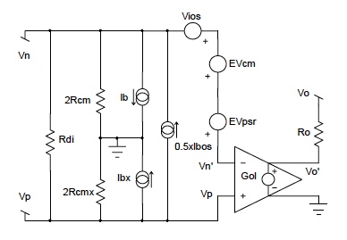
Figure 1: Op Amp Model with Error Parameters
Next in this experimental scenario, replace the DC voltage source Vx with a time varying voltage which does not increase without bound. Eventually, in some time Tfinal , thermal equilibrium will again be established. If this equilibrium condition establishes the same temperature Tx as reached before with the applied DC voltage Vx, then one can say that the "effective" value of this time varying function is Vx.
Hence the definition of "effective value".
DEFINITIONS
- Rdi is the differential input resistance between positive and negative input terminals. It is typically large enough to neglect in most practical situations; however, its value should always be examined. Data sheets specify input resistance as the resistance seen at one input with the other grounded. This data sheet parameter is Rdi in parallel with 2Rcm in Figure 1 and is essentially Rdi.
- Rcm is the common mode input resistance referenced to ground as seen by a common input source connected to both positive and negative inputs. This resistance is typically in the range of hundreds of megohms and generally neglected. Data sheets seldom give this value.
- Ro is the small internal output resistance as seen looking into the output terminal. In a voltage amplifier feedback topology with feedback factor "H", the effect of Ro is small (H*Ro/Gol) and is generally neglected.
- Ib (bias current) and Ibos (offset bias current) are associated with the positive (Vp) and negative (Vn) voltage inputs, which support input currents in a "live" topology. Input currents Ip and In are specified in data sheets via parameters Ib and Ibos. Equations 1 and 2 show the definitions relating data sheet items and actual Op Amp input currents.
- Vios (input offset voltage) is an internal IC device voltage error (referenced to the input) that relates output voltage for zero input. IC Op Amps have internal circuits that depend on matched devices. Perfect matching can not be achieved; therefore, a mismatch voltage error term exists as Vios in Figure 1. Note that an applied voltage equal to Vios between Vn, Vp such that the voltage between Vn', Vp is zero, forces the output to zero, neglecting all other error terms.
- PSRR, power supply rejection ratio, is responsible for a voltage error term referenced to the input, which relates changes in output voltage for changes in the IC supply voltages. The error term EVPSR in Figure 1 has a value of (PSRR* Δsupply voltage) for PSRRs given in data sheets as μV/V. PSRR may be given in dB for which EVpsr in Figure 1 is (Δsupply voltage * 10-PSRR/20 ).
- CMRR, common mode rejection ratio, determines a voltage error term referenced to the input, which relates the output voltage to a common mode voltage (Vcm) applied to both positive and negative inputs. Figure 1 shows this error term referenced to the input as EVcm. Equation 3 illustrates how this error term is calculated.
Current sources in Figure 1 support these equations.
ERROR BUDGET CALCULATIONS
The technique used in calculating impacts of error terms for a given application topology begins by using Figure 1 in a specific application topology and solving for the analytical output voltage (Vo) expression using Eqn 4, which neglects Ro.
Where Vp is the external voltage on the positive input as determined by the application topology and Vn' is the negative external input voltage (Vn) as determined by the application topology plus the accumulated internal errors.
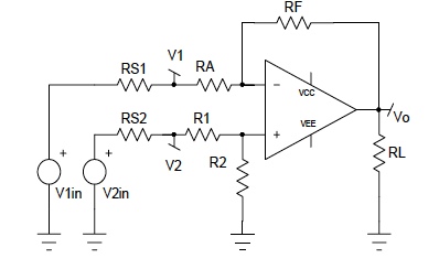
Figure 2: Single Stage Difference Amplifier
Figure 2 is the difference amplifier topology chosen for analysis in this Application Note because it is particularly vulnerable to resistor tolerances. Errors dominated by external resistor tolerances may justify a topology change; therefore, errors due to external resistors should always be examined first before internal IC errors are analyzed.
RS1 and RS2 are the source resistors for input source voltages V1in and V2in respectively. Often users forget to include these resistors when considering a specific application. When these resistors are large compared to RA and R1, they cause additional errors. Later in this Application Note, a topology will be recommended in which the impact of source resistors is diminished.
For now, assume the input voltage sources are near ideal (i.e. RS1=RS2=0). Using concepts embodied in Eqn 4, the output voltage (Vo) in Figure 2 is illustrated by Eqn 5.

Where terms Gn and Gp are the negative gain and positive gain respectively as shown;
The terms Rcm, Rdi, RS1, RS2, and Ro are neglected in deriving Gp and Gn in Eqn 5.
and if RA=R1, RF=R2; then Eqn 5 becomes the classic difference gain equation shown in Eqn 5a.

It is clear that mismatches in {RA; R1} and {RF; R2}, can cause errors; moreover, Eqn 5a is less correct if,
Note: Equations 5, 5a conform to the general feedback equations; namely,
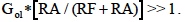
Gain closed loop =Gol/(1+Gol*H); where H is the voltage feedback factor and Gol is the amplifier open loop gain. For Gol*H>>1, Gain closed loop ≅1/H.
Gain Error due to Resistance Tolerance
Table 1 illustrates how resistor tolerances in Figure 2 impact the circuit gain for a random lot with open loop gain (Gol) constant. Note that the net percent error due to resistor tolerances alone can be very significant in this topology.Next after examining the variations in gain due to resistor tolerance, the effects of CMMR, PSRR, Vios, Ib, and Ibos are analyzed. The following error calculations are derived with; Eqns 3,4,and 5; V1=V2=zero; Rdi, Rcm, Ro, RS1, RS2 neglected; and
Throughout all these calculations RF=R2 and RA=R1.
Internal Offset Voltage (Vios) Error
The output voltage error caused by an Op Amp's internal mismatch voltage error term Vios is shown in Eqn 6 for the topology of Figure 2, using the Op Amp error model in Figure 1.
The Vios term is always shown in data sheets as a positive value; however, it is randomly either negative or positive.
Input Current Error
Input currents Ip and In on both the positive and negative inputs flow through the DC Thevenin Resistance associated with each input and develop unwanted voltages, which are amplified by the application topology. Eqn 7 shows this error for the topology in Figure 2, using the error model in Figure 1 with Eqns 1, 2.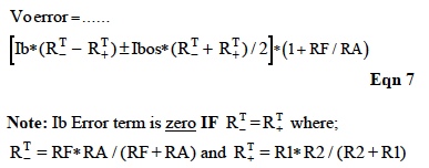
Reminder: Input Ib on data sheets is positive (into) for "n-type" devices and negative (out) for "p-type" devices; however, Ibos is always randomly either positive or negative.
CMRR Error
As previously discussed internal mismatches in the Op Amp cause output errors. Another example of this type error is the term EVcm, which is referenced to the input in Figure 1. The associated output error due to this term is shown in Eqn 8 for the topology in Figure 2.
Note: In Figure 2, one can assume that the external voltage between Op Amp inputs is essentially zero. Therefore, any Thevenin voltage on the Op Amp positive (+) input is essentially the common mode voltage (a quick trick to identifying, Vcm^T).
PSRR Error
Another error due to Op Amp internal mismatches is an output voltage change for changes in the power supply voltages. Figure 1 shows this error term referenced to the input as EVpsr. Equation 9 is the output error voltage for an Op Amp PSRR given in data sheets as μV/V.
When PSRR is given in dB, Eqn 9 becomes;

Example of Typical Error Calculations
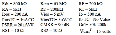
Typical Op Amp values for the difference amplifier topology of Figure 2 at 25° C is shown below. Change in power supply voltage is assumed to be 500mV.
Individual error calculations
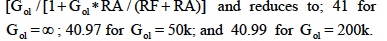
Most parameters have temperature coefficients (TC), which should be examined. The following calculations use only the TC values for Vios, and Ibos. The temperature multiplier is TC*(Ta −25°C). The term (Ta) is ambient temperature and limited to 40°C.In this example, input referenced error terms are multiplied by the closed loop gain, which is given as
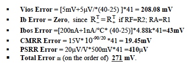
These calculations are not precise; nonetheless, this approach predicts error magnitudes and illustrates the most dominant parameter, Vios in this case. Clearly this particular configuration is not suitable for low-level dc measurements; for example, measuring current with a 100 ampere, 50mV resistance shunt (500μΩ )
Table 2 illustrates how error parameters in Figure 1 impact the total output voltage for the difference amplifier in Figure 2.
Single Stage Difference Amplifier Observations
The above analysis of Figures 1,2 shows;- Resistor tolerances do cause serious errors.
- Thevenin resistance at each (±) input should be equal
- Avoid high Vcm voltages.
- Input source resistors RS1, RS2 should be zero or RS1 much less than RA and RS2 much less than R1.
- Op Amp open loop gains (Gol) should be very high.
- Avoid large ambient temperature swings.
The Instrument Amplifier
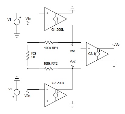
Figure 3: Basic Instrumentation Amplifier Topology
In calculating the overall gain for this topology, amplifiers G1, G2, are assumed to be near ideal with G3 an ideal unity gain amplifier. Specifically Ro, Rdi, Rcm, and error parameters in Figure 1 are neglected. The output stage G3 is typically the difference amplifier of Figure 2.
Equation 10 is the ideal expression for output voltage.
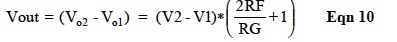
It is interesting to examine the effects Op Amp gains and non-identical RFs. This can be achieved by writing two node equations at Vn1 and Vn2, then solving for Vo1 and Vo2. Equation 11 illustrates the results.
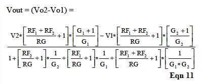
Although the gains (G1,G2) may not be equal, they can be assumed very large numbers and, therefore, set to a single very large gain (G) in Equation 11. In addition, if this gain (G) is >>> than [(RF1+RF2)/RG +1], then Equation 11 becomes;
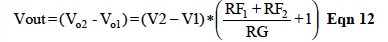
Note: The single resistor (RG) is responsible for changing gains of an Instrument Amplifier since RFs are internally fixed in the die. Moreover, the matching of RFs is usually so close that Equation 10 is valid. Furthermore, if the TC of RG and RF match, then the instrument amplifier gain expression is essentially independent of temperature.
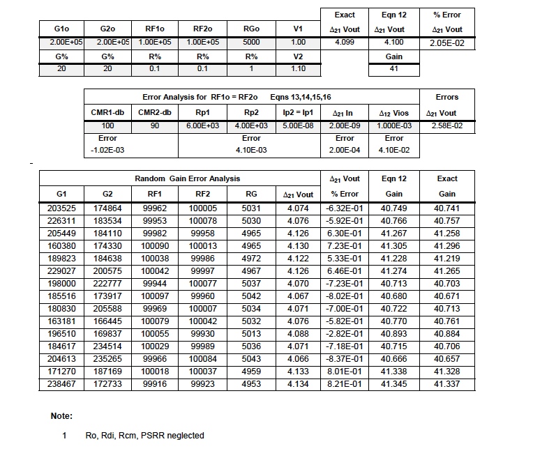
Table 3 illustrates how random values of gain and resistor values can impact the instrumentation amplifier net gain.
The error parameters of the Op Amp shown in Figure 1 cause output errors in an Instrument Amplifier. Errors are analyzed here to obtain first order approximation (FOA) insight into how they impact the output. The analytical process begins by substituting the model of Figure 1 for the amplifiers G1 and G2 in Figure 3.
Some reasonable assumptions are made to ease the math burden but not mask the dominant impact caused by error parameters.
These assumptions are;
- neglect Rdi, Rcm, and PSRR,
- resistors RP1, RP2 (source resistors of V1in and V2in) exist in the two input lines,
- Ip1, Ip2 are the two input currents and assumed equal to Ip (illustrates the effects of Rp1≠Rp2),
- CMRR1CMRR2; Vios1≠Vios2; Ibn1 ≠ Ibn2,
- RF1 = RF2; G1 = G2 = G,
- Inputs V1 and V2 are the common mode voltages (Vcm) on amplifiers G1 and G2 in Figure 3, and
- G3 in Figure 3 is an ideal unity gain amplifier.
Instrument amplifier major errors are due to external topology and the front-end Op Amp cells G1 and G2. The error equations shown below neglect non-zero errors in G3 (difference cell). These equations are presented to illustrate the impact of external application topologies.
These assumptions predict (Vo2-Vo1) errors as follows;
Note: Instrument Amplifier CMR is specified in data sheets as a net quantity, which includes the effect of all internal gain cells. Table 3 illustrates the impact of error parameters on the output voltage of the instrument amplifier in Figure 3.
Premium IC instrumentation amplifiers have well matched front-end Op Amps (G1,G2); consequently, Eqns 13 and 15 reduce to near zero. Moreover, if the engineer ensures an application, which has Rp1=Rp2, then Eqn 14 reduces to near zero. Instrumentation amplifiers with high CMR in cells G1,G2, and G3 minimize the impact of Eqn 16.
Clearly the Instrumentation Amplifier is a superior conditioning and instrumentation front-end topology compared to the single stage difference topology. Unfortunately, instrumentation amplifiers are not completely error free. Manufactures of Integrated Circuit (IC) Instrumentation Amplifiers do specify in their data sheets a set of net "error" terms, which apply to the total IC amplifier. For example; Vios, CMR, Ib, Ibos, Rinputs, etc are all specified as net device terms.
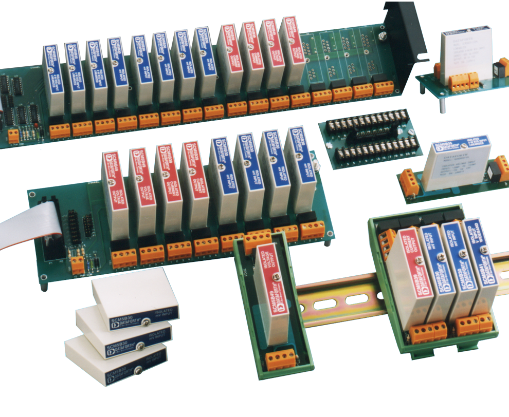
DATAFORTH MEASUREMENT DEVICES
Integrated circuit operational amplifier internal error terms do cause circuit topology dependent errors. Dataforth design engineers are imminently aware of these phenomena and use every available technique to minimize the impact of these error components on Dataforth's products. For example, Dataforth uses only premium IC's in their design together with unique patented circuit topologies to minimize errors. Moreover, all Dataforth modules are thoroughly tested and subjected to a thermal burn-in. In addition, internal voltage offset errors and gain errors due to resistor tolerance are removed by individual tuning on each module. Consequently, Dataforth has developed a quality cost effective product line of signal conditioning modules. The following are just a few of Dataforth's outstanding module benefits;- Dataforth signal conditioners use high performance amplifiers internally, which have low offset voltages (Vos) and low Vos TC. Residual errors due to Vos internal errors are calibrated out prior to shipment.
- Zero and Span errors caused by internal resistor tolerances are calibrated out prior to shipment. High performance amplifiers and discrete components ensure low drift over the wide operating range of -40C to +85C. Dataforth's amplifiers and associated adjustment networks provide stable calibration; therefore, after the modules are sealed no periodic calibrations are required.
- All Dataforth circuitry is designed to be insensitive to variations in power supply voltage. SCM5B modules operate over 4.75V to 5.25V with a power supply rejection (PSR) as low as 2uV per % variation in supply voltage, referred to input. SCM7B and DSCA modules operate over a much wider supply voltage range of 14 to 35V with PSR as low as 0.0001% of output per % variation in supply voltage.
- High input impedances (50 Meg ohms for 5B30-xx modules and 200 Meg ohms for 5B40-xx modules) allow interfacing to sensors with high output impedance. The use of FET input amplifiers result in low bias currents of 0.5nA, benefiting the user in allowing interfacing to sensors with high output impedance.
- Dataforth's patented unique iso-chopper isolation barrier allows continuous input common mode signal levels up to 1500Vrms (2200V peak). Common Mode Rejection of up to 160dB ensures signal integrity in extreme applications.
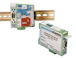
As an example consider measuring steady-state line current of a three-phase 3-wire delta connected AC motor using Dataforth's SCM5B40/41 wide bandwidth analog voltage module and a four-wire shunt sensor. Figure 4 illustrates the modular structure of Dataforth's SCM5B40/41 used in this example. Three phase line current shunt measurements on delta 3-wire devices must be done with low voltage (typically 50mV) shunts to maintain balanced load conditions. Such low voltage measurements require accurate modules, which must maintain accuracy at common mode voltages equal to AC line values.
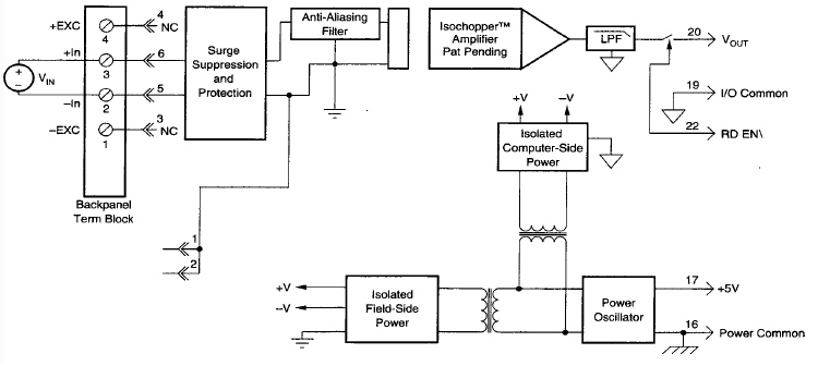
Figure 4: Dataforth SCM5B40/41 Isolated Analog Module
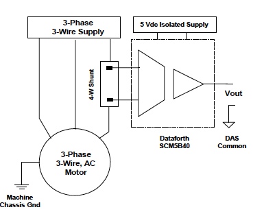
Figure 5: 3-Phase Line Current Measurement
Figure 5 illustrates a line current measurement for a 100 horsepower 3-phase 460 volts AC (126 A rms full load), 60 Hz delta connected motor. Dataforth's SCM5B40-02 module (output −5 to +5 volts, input −50mV to +50mV, gain 100V/V) is used to sense line current in a 300A, 50mV, 166.667μΩ shunt. Shown below are error calculations using Dataforth's specifications. See Dataforth's AN104 for more specification details.
- Input Resistance: 200MΩ ,40kΩ off/overload This has insignificant effect on the net Rshunt resistance.
- CMV: 100 dB (1500Vrms input/output max). Common mode voltage input/output is 267 (462÷√3) Vrms, for this balanced motor with negligible IR drops in the building ground structure. The error is 267V*10^(-100/20) = 2.67 mV rms. See AN103 on CMR.
- Power Supply Sensitivity: 2μV/% RTI. The error is ±2μV/%*5%*100V/V = ± 1mV rms, for a 5% variation in the 5 volt module power supply.
- Input Bias Current: ±0.5nA. The error is ±0.5nA*Rshunt*100V/V, certainly negligible.
- Accuracy: Includes nonlinearly, hystersis, and repeatability; (a) ±0.05% of Span; (b) ±10μV RTI; (c) ±0.05% of Vz. Errors are determined as follows;
- (±0.05%)*10V = ± 5mV rms ,
- ( ±10μV)*100 V/V = ± 1mV rms ,
- (±0.05%)*0mV =± 0 V rms (Vz =0 V)
- Stability: Input offset ±1μV/°C; Output offset ±40μV/°C; Gain ±25 ppm/°C of reading. For a temperature of 122°F, (25°C change from 25°C room), stability calculations in volts rms are;
- Input offset ±1μV/°C*25°C*100 V/V= ± 2.5mV
- Output offset ±40μV/°C*25° = ± 1mV.
- Gain 25 μV/°C*25°C*5 = ± 3.1 mV, max.
Random (±) terms will likely not be the same sign; hence, adding would give an unlikely net error. Another method for adding ± random mutually exclusive rms values is the square root of the sum of squares of each (±) term. This method gives an estimated net error of ± 7.14mV rms.
Table 1
Single Stage Op Amp Difference Amplifier Gain ErrorReference Figure 2
Table 1 is available on Sheet #1 of the interactive Excel Workbook. The reader is encouraged to download this Excel file http://www.dataforth.com/catalog/pdf/an102.xls , choose their own values, follow instructions, and examine the effects of their own selected resistor, gain, temperature, and tolerance values.
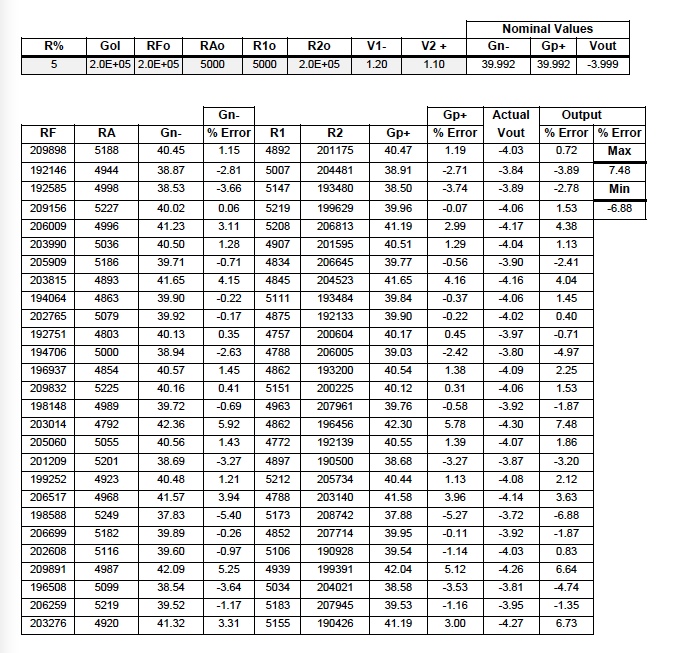
Table 2
Single Stage Op Amp Difference Amplifier Error Budget 1Reference Figure 1
Table 2 is available on Sheet #2 of the interactive Excel Workbook. The reader is encouraged to download this Excel file http://www.dataforth.com/catalog/pdf/an102.xls , choose their own values, follow instructions, and examine the effects of their own selected values.
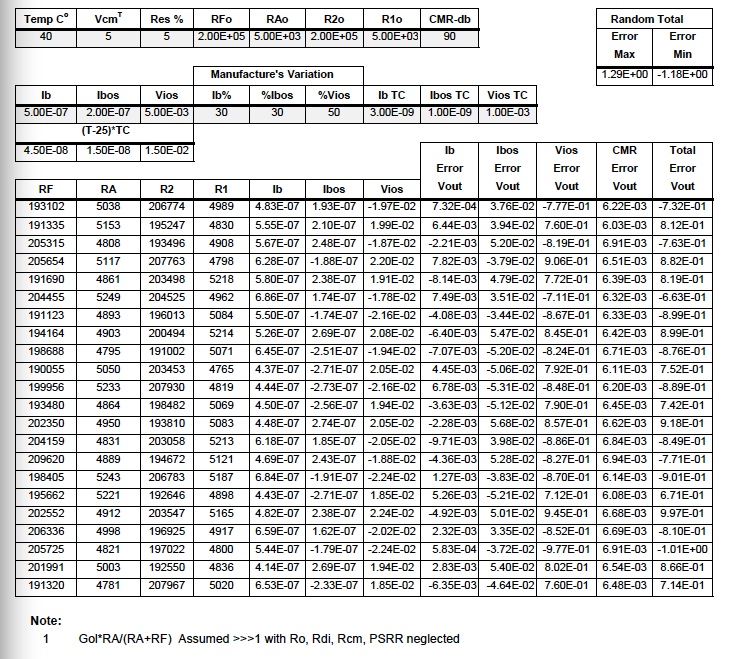
Table 3
Instrument Amplifier Error in Gain (2RF/RG+1) Including Error Parameter Analysis 1Reference Figure 3
Table 3 is available on Sheet #3 of the interactive Excel Workbook. The reader is encouraged to download this Excel file http://www.dataforth.com/catalog/pdf/an102.xls , choose their own values, follow instructions, and examine the effects of their own selected values
Was this content helpful?
Thank you for your feedback!